


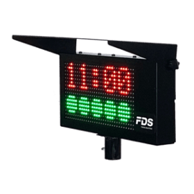

Nb8511-pcb-mb-v4 Boardview Guide
“Unless,” Maya said, pulling up the physical board and a microscope, “the dielectric between inner1 and inner2 on this particular batch was mis-specified. The fab house used a prepreg that’s half the required thickness.” She pointed to region D-17 on the boardview. “Look. Right under C442’s shadow. The 3.3V plane on inner1 and the GND plane on inner2 aren’t just overlapping—they’re perfectly aligned for a two-centimeter square.”
“The boardview wasn’t wrong,” Maya said, sitting back. “It was telling us the truth. We just didn’t know how to read it.”
He pulled up the file. The software rendered the board as a series of translucent layers: top copper in red, inner1 in green, inner2 in dark blue, bottom copper in yellow. Components appeared as ghostly outlines with pin-number labels. It was beautiful, precise, and utterly silent about what connected to what. nb8511-pcb-mb-v4 boardview
The fix was insane but simple: drill a tiny hole through the overlapping region to break the capacitive coupling, then backfill with non-conductive epoxy. It took three hours of microsurgery under a stereo microscope. When they powered up the board again, C442 stayed cold. The 3.3V rail held steady.
Dev looked at Maya. “You just diagnosed a short that didn’t exist in any netlist, any schematic, any continuity test. You diagnosed a ghost .” “Unless,” Maya said, pulling up the physical board
Dev stared. “You can’t overlap power and ground planes. That’s a capacitor the size of the whole board. It would oscillate like crazy.”
Maya saved the boardview file one last time. In the REV_NOTES field, she added a new line: “Hole drilled at D-17. Dielectric thickness critical. The map had the secret—you just had to believe it was there.” Right under C442’s shadow
Dev zoomed into C442. “Here. The little bastard. The boardview says its positive terminal is net ‘+3V3_MEM,’ and its negative is ‘GND_REF.’ That’s fine. But when I meter it, there’s zero ohms between those nets. So either the boardview is wrong, or the physical board has a solder bridge somewhere.”
“Show me the boardview again,” Maya said, leaning over Dev’s monitor.
“It’s like having a map of a city with no street names,” her lab partner, Dev, grumbled, rubbing his eyes. They’d been at it for fourteen hours. The boardview showed the physical location of every resistor, capacitor, and via on the four-layer PCB. But without the netlist—the logical connections—it was just a pretty picture of silkscreen and copper.
Dev leaned in. On the boardview, the two planes showed as overlapping translucent shapes, creating a muddy brownish color. He’d always assumed that was a rendering artifact.